Details
Part No: 04B-005
Title: Common Emitter Amplifier
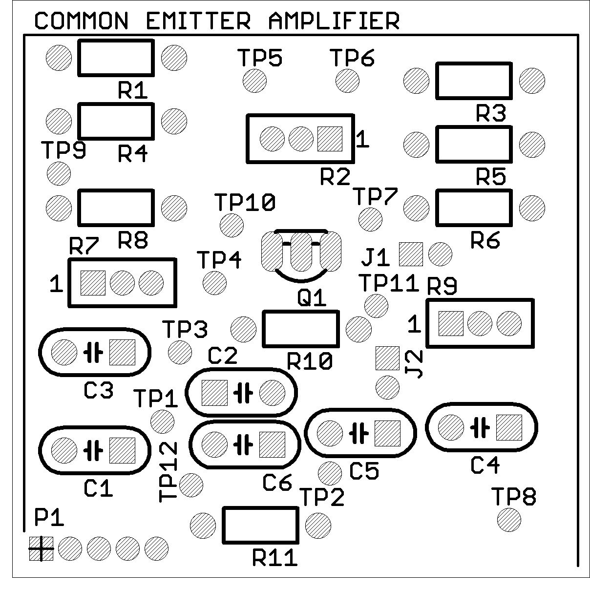
Board Size: 50 x 50 mm
Pieces per Panel: 4
Panel Size: 100 x 100 mm (V-scored)
Description
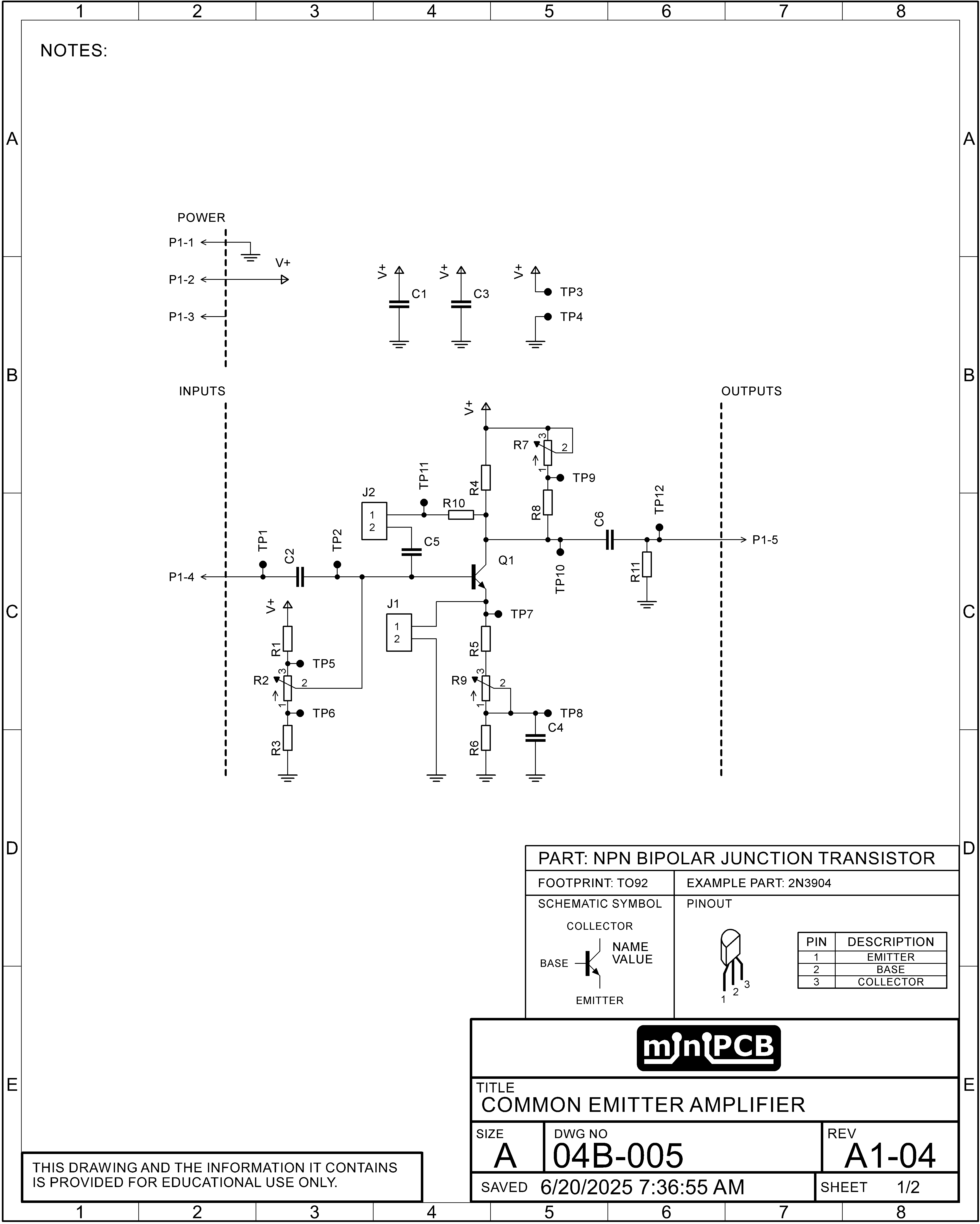
The 04B-005 Common Emitter Amplifier board is designed to provide a robust platform for amplifying analog signals, making it an essential tool for electronics experimentation and prototyping. This board is structured around a common emitter configuration, which is widely recognized for its ability to deliver significant voltage gain while maintaining a straightforward design.
At the heart of the amplifier is a transistor whose bias point is set by a combination of resistors R1, R2 (trimmer), and R3. These components play a crucial role in establishing the operating conditions of the transistor, allowing users to adjust the bias for optimal performance. The input signal is AC-coupled through capacitor C2, which effectively blocks any DC component, ensuring that only the desired AC signal is amplified. Measurement points TP1 and TP2 provide convenient access to the input signal and the transistor's base voltage, respectively.
Power rail decoupling is handled by capacitors C1 and C3, which stabilize the power supply and minimize noise. The output stage of the amplifier also features AC coupling via capacitor C6, ensuring that the output signal is free from DC offset. Measurement point TP12 allows users to monitor the output signal directly.
The feedback network, composed of C5, R10, and J2, can be disconnected to observe the amplifier's behavior without feedback influence. Similarly, the feedback and biasing network formed by R5, R6 (trimmer), R9, C4, and J1 can also be bypassed, providing flexibility in testing and design. Measurement points TP7 and TP8 facilitate the analysis of this feedback network, while TP11 offers insight into the interaction between C5 and R10.
For practical testing, typical resistor values in the biasing and feedback networks can vary, impacting the amplifier's gain and bandwidth. Higher resistor values may lead to increased noise sensitivity, while lower values can enhance stability but may limit gain. Users should consider these trade-offs when selecting component values to tailor the amplifier's performance to specific applications. Overall, the 04B-005 board is an invaluable resource for those looking to explore the principles of amplification in electronic circuits.
Schematic
Layout
Videos
Downloads
Additional Resources
Revision History
| Date | Revision | Description | By |
|---|---|---|---|
| 2024-12-03 | A1-01 | Initial Release | N. Manteufel |
| 2025-04-30 | A1-02 | Updated PCB outline, removed logo. | N. Manteufel |
| 2025-06-30 | A1-03 | Added AC coupling capacitors to output. | N. Manteufel |
| 2025-06-30 | A1-04 | Moved R9 in circuit. | N. Manteufel |