PCB Details
Part No: 04B-350
Title: Cascode Cascade Amplifier
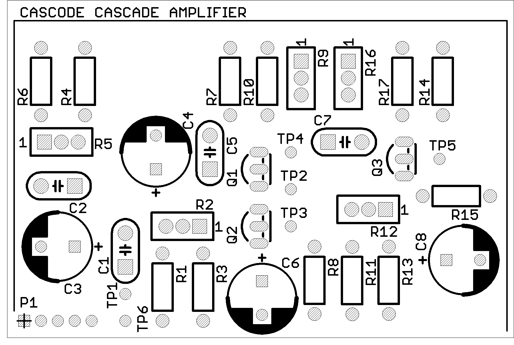
Board Size: Approx. 75 x 50 mm
Pieces per Panel: 2
Panel Size: 75 x 100 mm (V-scored)
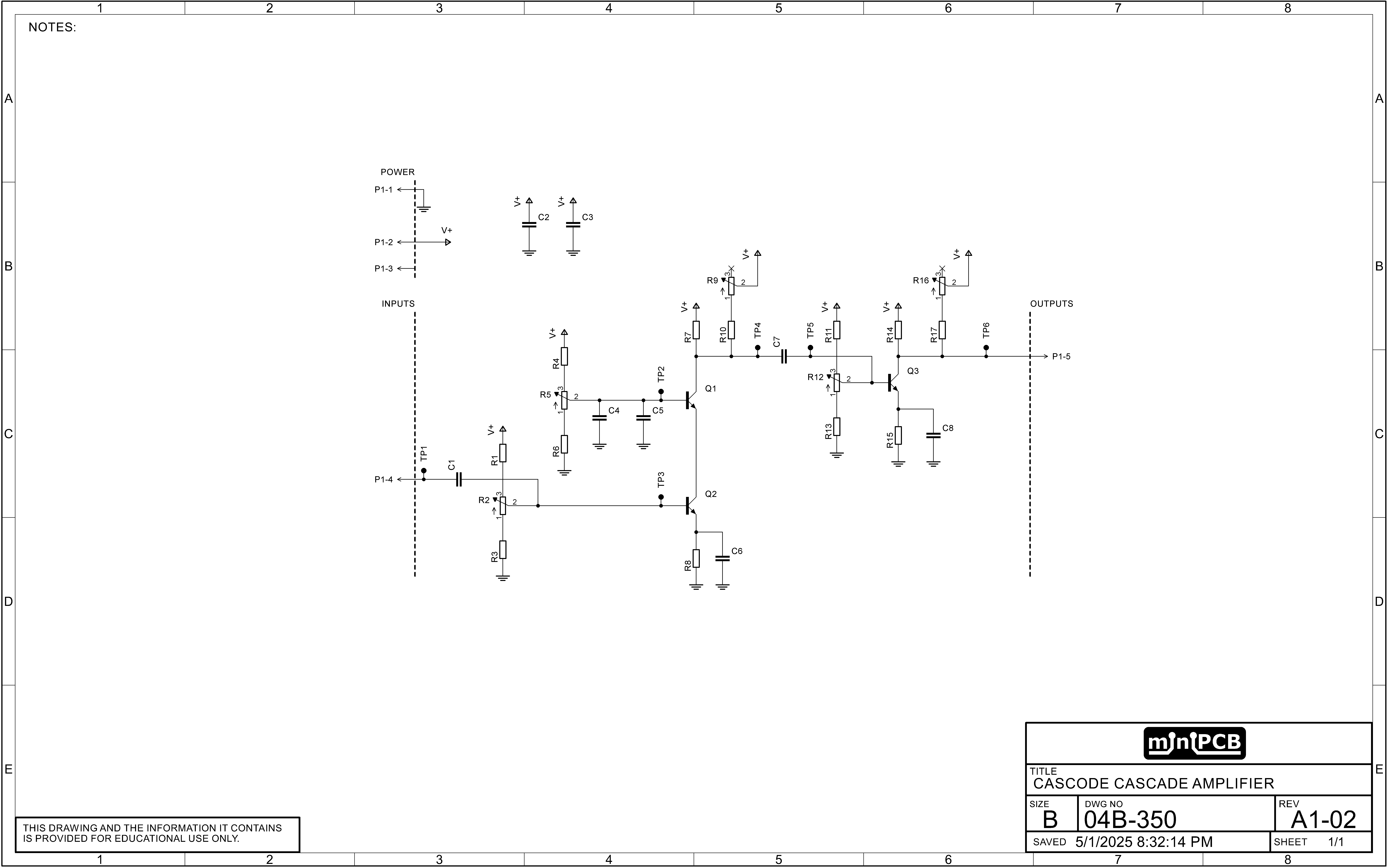
This miniPCB implements a three-transistor cascode-cascade amplifier designed to combine the high-frequency advantages of a cascode stage with the voltage gain stacking of a cascaded configuration. Built around discrete NPN bipolar junction transistors (Q1, Q2, and Q3), the circuit enables hands-on exploration of advanced analog amplifier techniques including stage isolation, Miller effect suppression, and gain distribution.
Power Supply Conditioning
Capacitors C2 and C3 act as power rail filter capacitors, suppressing high-frequency noise and stabilizing the DC supply voltage. Test point TP4 allows measurement of the collector of Q1, providing insight into the voltage swing of the cascode stage output.
Input Coupling and Signal Entry
The input signal is AC-coupled via C1, which decouples the DC component of the input source and ensures proper biasing of the first active stage. Test point TP1 enables measurement of the input voltage directly at the signal entry.
Cascode Input Stage (Q2)
Q2 serves as the lower transistor in the cascode configuration. Its base is biased using a resistor network composed of R1, R2 (a multiturn trimmer), and R3, which set the operating point and collector current. Test point TP3 provides access to the base of Q2 for bias voltage monitoring.
The emitter of Q2 is connected to ground through R8 and capacitor C6, forming an AC ground while providing emitter degeneration and thermal stability.
Cascode Driver Stage (Q1)
Q1 operates as the upper transistor in the cascode pair, with its emitter directly connected to the collector of Q2. Its base is biased by a network of R4, R5 (trimmer), and R6, while capacitors C4 and C5 stabilize this bias voltage by bypassing transient variations. Test point TP2 enables voltage measurements at the base of Q1.
The collector of Q1 connects to the V+ rail through R7, R9 (trimmer), and R10, which set the collector load and influence the gain. TP4, as previously mentioned, monitors this node.
Cascaded Amplifier Stage (Q3)
The output from the cascode stage is AC-coupled to the next gain stage via C7, which connects the collector of Q1 to the base of Q3. This decoupling capacitor allows signal transfer while maintaining DC bias separation between stages. Test point TP5 enables direct measurement of the Q3 base.
The base of Q3 is biased by a resistor divider made up of R11, R12 (trimmer), and R13. The emitter is grounded through R15 and bypassed by C8 to reduce AC degeneration and improve gain. The collector load is formed by R14, R16 (trimmer), and R17, connected between the collector and V+. Test point TP6 enables probing of the Q3 collector and serves as a convenient output node for scope or load connection.
Transistor Configuration and Application
Q1 and Q2 form a cascode stage, where Q2 handles the input signal and Q1 buffers the output, enhancing bandwidth and reducing distortion. Q3 then cascades the amplified signal, offering additional gain. This layout is ideal for demonstrating stage-to-stage interaction, frequency response shaping, and biasing strategies in high-performance amplifier design.
Simulation
Schematic

Board Layout

Downloads
Coming Soon
We are working on additional resources for this PCB. Please check back later!