PCB Details
Part No: 04B-340
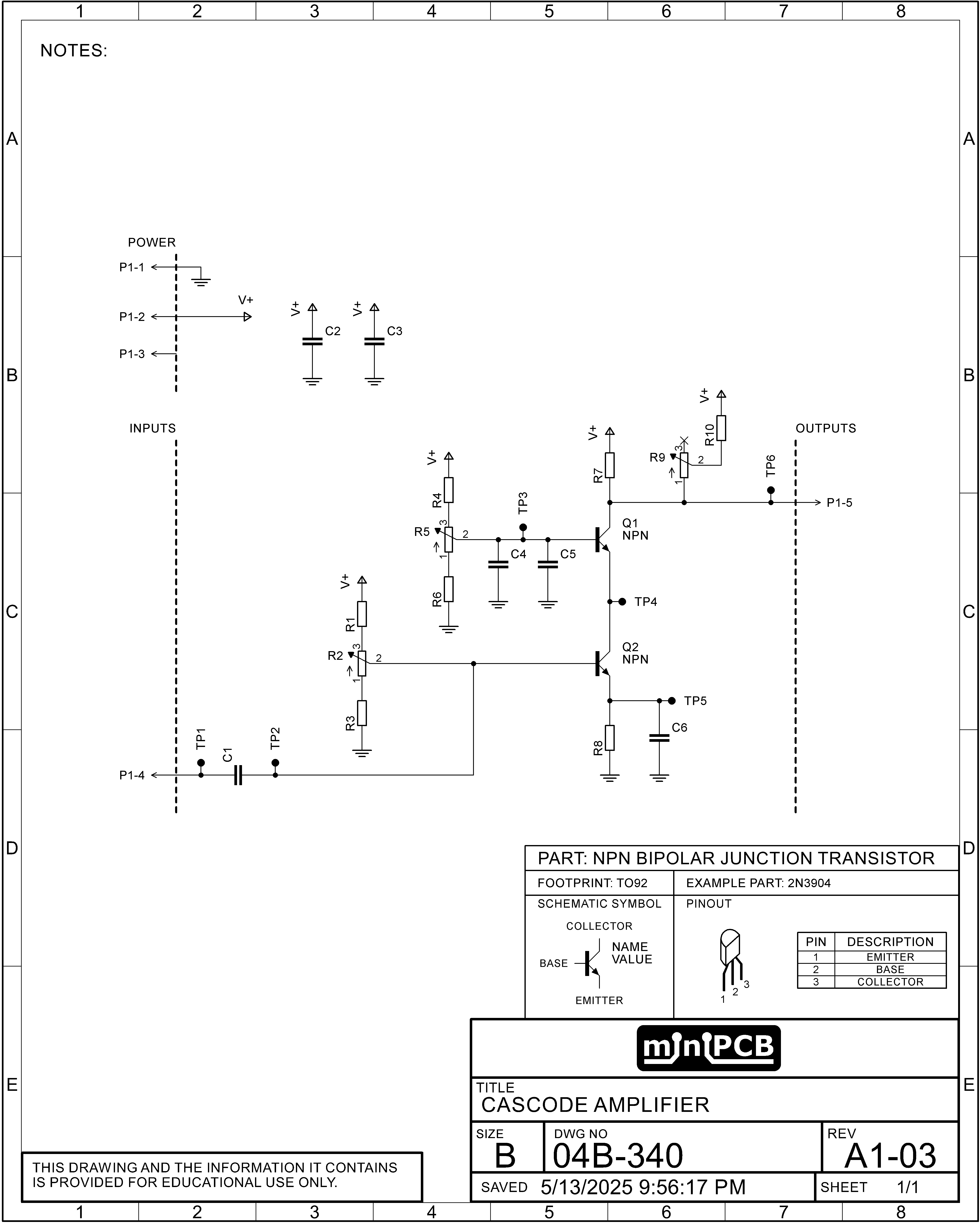
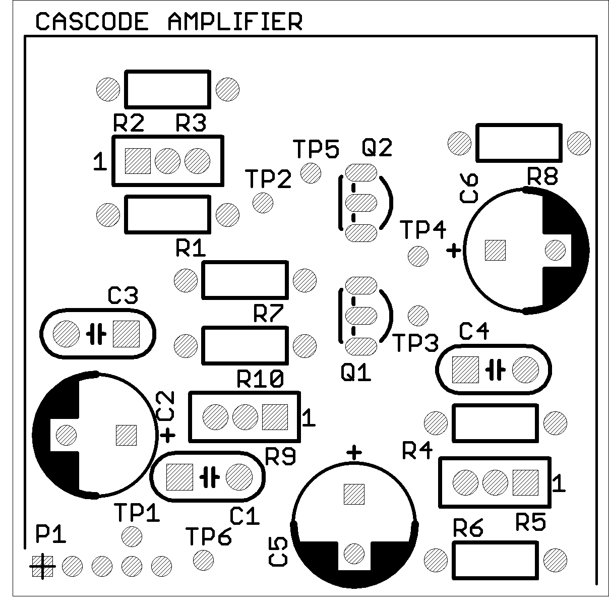
Title: Cascode Amplifier
Board Size: Approx. 50 x 50 mm
Pieces per Panel: 4
Panel Size: 100 x 100 mm (V-scored)
This miniPCB implements a single-stage cascode amplifier using two discrete NPN bipolar junction transistors (Q1 and Q2) in a stacked configuration. The design can optionally accommodate N-channel MOSFETs in place of BJTs for comparative testing. The cascode topology combines a common emitter (Q2) and common base (Q1) stage to achieve high voltage gain, increased bandwidth, and improved isolation between input and output. This circuit is ideal for demonstrating the performance advantages of cascode operation, including reduced Miller effect and enhanced high-frequency response.
Input Coupling and Biasing – Q2 Stage
The AC input signal is coupled to the circuit through C1, a DC blocking capacitor that prevents source bias from interfering with the transistor's base. The input transistor Q2 is biased via a voltage divider consisting of R1, R2 (a multiturn trimmer), and R3, allowing precise adjustment of the base voltage and establishing the correct quiescent current. TP2 allows direct measurement of Q2’s base voltage, while TP1 monitors the input signal level.
Power Supply Filtering
C2 and C3 are supply rail filtering capacitors that stabilize the positive voltage rail and suppress high-frequency noise. These components improve power integrity for both gain stages.
Biasing of Q1 – Common Base Stage
The base of the output transistor Q1 is held at a fixed voltage determined by a voltage divider formed by R4, R5 (a multiturn trimmer), and R6. This sets the operating point for the common base stage. C4 and C5 are connected in parallel with the base bias node to stabilize the voltage and filter out noise or ripple, ensuring stable operation. TP3 allows direct probing of Q1’s base voltage.
Collector and Interstage Connection
Q2’s collector is directly connected to the emitter of Q1, forming the critical cascode connection between stages. TP4 is placed at this node to measure the intermediate collector-emitter junction between the two transistors. This connection minimizes voltage variation at Q2’s collector, significantly reducing Miller capacitance and improving high-frequency gain.
Emitter Network – Q2 Stage
The emitter of Q2 is connected to ground through R8, providing a path for emitter current, while C6 is placed in parallel to allow AC signals to bypass the resistor and maintain high gain at signal frequencies. TP5 enables direct measurement of Q2’s emitter voltage for DC bias or signal monitoring.
Output Stage – Q1 Collector
The collector of Q1 forms the output of the amplifier and is connected through a resistive load composed of R7, R9 (a multiturn trimmer), and R10. This network determines the output voltage swing and affects overall gain. Fine-tuning via R9 allows adjustment of the output bias point. TP6 allows measurement of Q1’s collector voltage, which represents the final output signal of the amplifier.
Transistor Configuration
Both Q1 and Q2 are mounted in TO-92 footprints with a standard C-B-E (Collector–Base–Emitter) pinout. The layout is optimized for NPN BJTs, though many N-channel MOSFETs with matching pinouts are also compatible and can be used for substitution and experimentation. Most JFETs are not drop-in compatible due to differing pinouts and biasing requirements. This flexible design allows users to explore the advantages and tradeoffs of different transistor types within the cascode configuration.
Schematic

Board Layout
